

Our related videos

-
- Ultra Thin 2L-FCCL
Sputtering method Flexible Copper Clad Laminate - Super Thin Copper Foil for IC substrate
- R2R Magnetron Sputtering Metallized Thin Film Service
- Copper Foil sputtered Graphite Thermal Film
- IC Heat Spreader
- R2R Nickel Coated Film (Nickel Plated Film)
- Ultra Thin 2L-FCCL
-
Super Thin Copper Foil for IC substrate
Product Instruction:
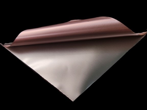
■ Super Thin Copper Foil for IC substrate is 3um copper which covered with 18um copper foil. It is extremely easy to peel off once apply.
■ Suitable for mSAP semi-additive process, can be used as thin circuit substrate application.
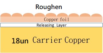
■ The metal releasing layer + 3um electroforming copper is generated by physical production procedure on 18um copper foil substrate.
■Suitable for IC Substrate, high-density interconnect technology boards, IC package process materials, etc.
■ Comply with RoHS and Reach specifications
Super Thin copper foil with carrier is mainly used for IC Substrate which are formed by MSAP process.
The thickness of ultra-thin copper foil for IC Substrate is generally between 2um and 5um. In the initial stage, Topnano’s Super Thin Copper Foil for IC Substrate products will mainly be 3um products for promotion and use.
Topnano's Super Thin Copper Foil for IC Substrate is made up of 18um carrier copper foil and peelable ultra-thin copper foil.
Generally, after laminating the adhesive film on the copper carrier board, the customer will remove the 18um copper carrier foil, leaving only the ultra-thin peelable copper in the IC Substrate to be used as the copper seed layer.
In recent years, as IC component functions have become more complex, the number of board layers used has increased.
If end-products continue to move toward thinner and lighter designs, the limited space inside the equipment will drive more PCB processes to use ultra-thin copper foils.
In addition to the layering process, the copper-clad substrate, which is the core layer, may also use ultra-thin copper foil in the future to satisfy the trend of equipment thinning.
Application:
Ultra-thin copper foil (2-5 micrometers) with a low roughness Rz < 2 is primarily used in high-end PCB manufacturing, especially in products requiring high-speed, high-frequency signals and fine-grained circuitry. Potential applications include:
• High-density interconnect (HDI) circuit boards: Ultra-thin copper foil enables finer circuit designs, improving circuit density and performance, suitable for high-end electronic products such as mobile phones and communication equipment.
• IC substrates and coreless substrates: Low roughness provides excellent electrical performance and signal integrity, suitable for flip-chip packaging and other high-frequency, high-speed applications.
• 5G and high-speed communication equipment: Ultra-thin and low-roughness copper foil reduces signal loss, improves the quality of high-speed signal transmission, and meets the requirements for high-frequency, low-loss substrates.
Ultra-thin copper foil is suitable for carrying currents below 5 amps, with lower electrical load requirements, but is suitable for applications with high demands for fine circuitry, high-frequency and high-speed signals, and minute dimensions.
Downstream applications include: memory (DRAM, NAND), smart phone AP, power management IC, IC package loading board of RF module, etc.
In summary, ultrathin copper foil with Rz<2 exhibits superior performance in high-speed, high-frequency, and miniaturized electronic products, and can support more refined circuit processes, making it one of the key materials for future advanced electronic manufacturing.
Composition
*Interested in the product, please contact us Email: joe_lin@topnano.com.tw (Mr. Lin)*
Usage (for reference only)
In PCB manufacturing process, 18um copper foil is laminated with various resin substrates including Prepreg to form CCL, and then the 18um copper foil is torn off.
In PCB manufacturing process, after etching process to make the proper circuit, then press the 18um carrier copper foil with Prepreg or other resin substrate to form CCL, and then separate the 18um carrier copper foil.
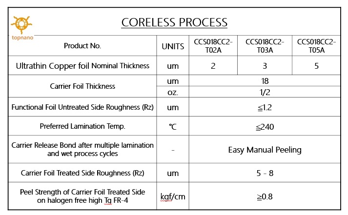
Representive dataThe Spec detail of Super Thin Copper Foil for IC substrate
Topnano’s Ultrathin copper foil for Coreless Process
Topnano’s Ultrathin copper foil for MSAP Process
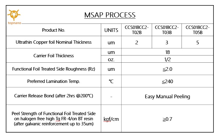
※The above table is representative data and not guaranteed.
※Peel Strength is the test value after plating to 35um thickness.
※Currently, there are two types of products available: Glossy copper foil without roughening / Matte copper foil with roughening.
※The carrier copper foil is fixed at 18um copper foil, and the ultra-thin tearable copper can be customized from 1.5um to 5um according to customer's needs.1.5um~5um
More knowledge about ultra-thin copper foil and mSAP process:- Advantages of ultra-thin copper foil and mSAP process for manufacturing fine-line circuits on IC carrier boards
- Copper Foil Surface Roughness and Its Impact on PCB and 5G High-Speed Transmission
- PCB Copper ED Copper vs Ra Copper vs Sputter with Plating Copper
Optimal Use Period :
Within 6 months from the shipment date indicated on the order.