


Our related videos

-
- Ultra Thin 2L-FCCL
Sputtering method Flexible Copper Clad Laminate - Super Thin Copper Foil for IC substrate
- R2R Magnetron Sputtering Metallized Thin Film Service
- Copper Foil sputtered Graphite Thermal Film
- IC Heat Spreader
- R2R Nickel Coated Film (Nickel Plating Film)
- Ultra Thin 2L-FCCL
-
Sputtered Method Ultrathin Copper FCCL (2L-FCCL)
2L-FCCL Adhesiveless Two-Layer Flexible Copper Clad Laminate
Fineline Flexible Printed Circuit Board Material with Low Surface Roughness
Topnano's 2L-FCCL (Two-Layer Flexible Copper Clad Laminate) is an adhesive-free composite material. Using high-heat-resistant PI (polyimide) or PET film as the substrate, it directly deposits an ultra-thin copper layer of 2–18 µm using roll-to-roll vacuum magnetron sputtering technology and copper plating thickening equipment.
This composite material features a low-roughness copper layer, high peel strength, and high heat resistance, and is widely used in high-end products such as printer FPCs, 5G communications, flexible displays, FPC antenna , EMI electromagnetic shielding films, automotive electronics, and medical-grade flexible sensors.Sputtered FCCL Product Features:
-
Key Material for Flexible Printed Circuit & Rigid-Flex Boards: This product serves as one of the primary upstream materials for both Flexible Printed Circuits (FPC) and Rigid-Flex boards.
-
Adhesive-Free 2-Layer FCCL: Our 2-layer FCCL is free from adhesive between the PI (Polyimide) and copper, making it ideal for advanced FPC manufacturing, including Fine Line FPCs and tape COF FCCLs.
*Customers can provide their own PET Film to our company for copper plating to make customize PET FCCL.
-
Low Roughness FCCL: Sputtered FCCL has a very fine grain structure in its copper layer, and the surface roughness(Rq) is only about 13nm, which is much lower than that of traditional electrolytic copper and rolled copper.
-
Advanced Manufacturing Process: Produced using Roll-to-Roll vacuum sputtering and chemical electroforming (electroplating) processes, ensuring high-quality copper layers.
-
Versatile Copper Thickness: With copper thickness ranging from 2μm to 8μm, our FCCL is suitable for Fine Line layout designs. The single-sided copper layer can be extended up to 9μm to 18μm.
-
Peel strength: FCCL peel strength can reach > 0.7kgf/cm (Depending on the choice of seed layer and PI substrate)
The bonding strength between the copper layer and the substrate is sufficient -
Customizable for Thick Copper Applications: For customers needing FCCL with copper thicker than 18μm, our 8μm FCCL product can be further plated with copper to achieve the desired thickness.
-
Optimized for mSAP Modified Semi-Additive Process: This FCCL supports the mSAP process for flash etching, minimizing lateral etching and reducing etching time.
-
Ideal for PCB Circuit Boards: Our 2μm FCCL products can also serve as semi-build-up materials for PCB circuit boards, acting as a metal seed layer (metal conductor layer).
-
RoHS & Reach Compliant: This product meets the RoHS (Restriction of Hazardous Substances) compliance standards, ensuring it is environmentally friendly.
-
Recommended Etching Process: For etching, we recommend using Copper(II) chloride (CuCl2) Etching Liquid or laser engraving to create the required lines.
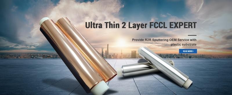
Sputtered FCCL Product Advantages:
◎Effectively reducing copper etching residues problems which normally happen on 3L-FCCLs.
◎Material characteristics are similar to ED Copper, but the etching time is shorter, which can save 20% of the etching time.
◎High heat resistance, fine flexural/bending endurance, good peel strength, copper layer uniformity, and dimensional stability.
Why Choose Our Sputter Type FCCL?
-
High-performance for advanced FPC applications
-
Flexible thickness options for diverse needs
-
Superior surface quality for enhanced conductivity
-
Environmentally friendly and compliant
-
Compatible with cutting-edge manufacturing processes
Target Customers & Solutions:- Customers troubled by current FCCL stack-up thickness and seeking thinner materials to meet lightweight electronic design trends.
- Customers using "selective copper plating" in Pattern Processes (our thin copper layer shortens process time and reduces undercut risk).
(Our FCCL copper layer is very thin, which can shorten process time and risk of undercut during patterning.)
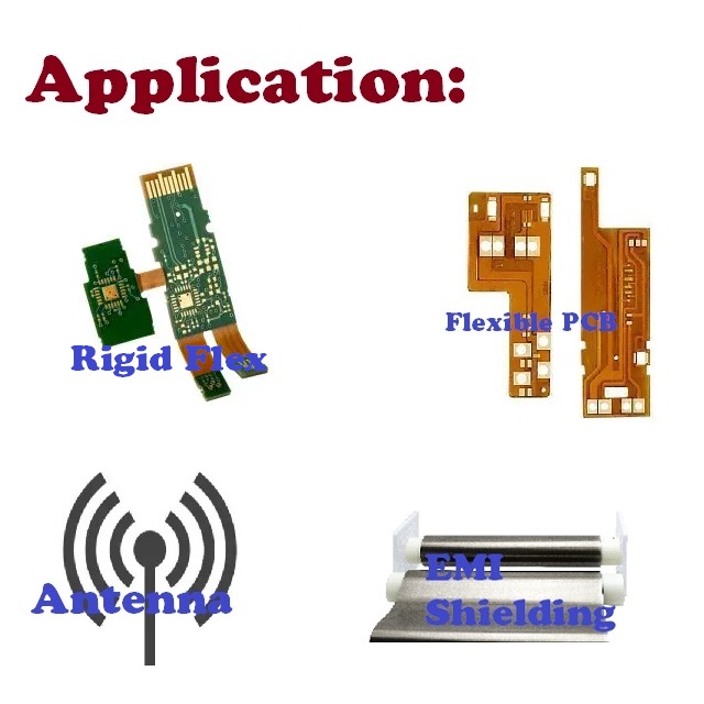
Sputtered FCCL Application (Final products):
*Wearable devices (smart watches, wireless bluetooth earphones, sports bracelets)
*Smart phones
*OLED display
*Smart Car devices
*EMI Shielding Film
*FPC Antenna
*5G Application products
*Internet of Things( IOT) Application products
*Polyimide film heaters (Thin Film Heater)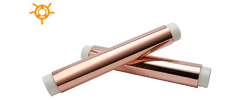
Knowledge & Applications ( Technical Articles):
-
Transparent LED Film Screen Circuit material 2Layer PET Copper Film
-
Copper Foil Surface Roughness and Its Impact on PCB and 5G High-Speed Transmission
-
Seed layer in the sputtering material plays a key role as the "glue"
-
Intro of Roll-to-Roll vacuum sputtering conductive materials (Cu/Al /ITO/ Graphite)
-
Sputtered FCCL helps you solve yield defects in chemical copper reduction processes
** For Each Spec Introduction and catalogue, please refer to <topnano in Taiwantrade> URL:https://topnano.en.taiwantrade.com>
*If you are interested in the product, please contact us Email: joe_lin@topnano.com.tw (Mr. Lin)*Sputtered FCCL Product Specifications
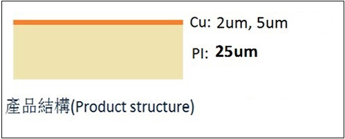
Ultra Thin FCCL (Single Side)
-
Single Side Item No.
-
PI Film
-
Cu layer
-
Width
-
Length
-
Item No.
-
FCS025KA1-T02
-
PI Film
-
25 um
-
Cu layer
-
2 um
-
Width
-
500 mm
-
Length
-
100~200M
-
Item No.
-
FCS025KA1-T05
-
PI Film
-
25 um
-
Cu layer
-
5 um
-
Width
-
500 mm
-
Length
-
100~200M
-
Item No.
-
FCS050DU2-T02
-
PI Film
-
50 um
-
Cu layer
-
2 um
-
Width
-
500 mm
-
Length
-
100~200M
-
Item No.
-
FCS050DU2-T05
-
PI Film
-
50 um
-
Cu layer
-
5 um
-
Width
-
500 mm
-
Length
-
100~200M
-
Item No.
-
FCS050DU2-T08
-
PI Film
-
50 um
-
Cu layer
-
8 um
-
Width
-
500 mm
-
Length
-
100~200M
-
-
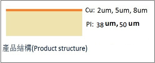
MOQ : 1 Roll (=100M)
Ultra Thin FCCL(Double Side)
-
Double Side Item No. -
PI Film
-
Cu layer
-
Width
-
Length
-
Item No.
-
FCD025KA1-T02
-
PI Film
-
25 um
-
Cu layer
-
2 um
-
Width
-
500 mm
-
Length
-
100~200M
-
Item No.
-
FCD025KA1-T05
-
PI Film
-
25 um
-
Cu layer
-
5 um
-
Width
-
500 mm
-
Length
-
100~200M
-
Item No.
-
FCD050DU2-T02
-
PI Film
-
50 um
-
Cu layer
-
2 um
-
Width
-
500 mm
-
Length
-
100~200M
-
Item No.
-
FCD050DU2-T05
-
PI Film
-
50 um
-
Cu layer
-
5 um
-
Width
-
500 mm
-
Length
-
100~200M
-
Item No.
-
FCD050DU2-T08
-
PI Film
-
50 um
-
Cu layer
-
8 um
-
Width
-
500 mm
-
Length
-
100~200M
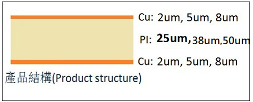
MOQ : 1 Roll (=100M)
-