


Our related videos

Knowledge
Seed layer in the sputtering film plays a key role as the glue function
The seed layer plays an important role in the sputtering process, which is a technique commonly used in the preparation of thin metal films. The seed layer is an extremely thin metal film, usually between a few nanometers and tens of nanometers thick, that is applied to the surface of the substrate as the starting point for the metal film.The seed layer has the following main functions in the sputtering process:
Increase Adhesion: The seed layer provides a good adhesion surface to ensure that the subsequent sputtered metal film adheres firmly to the substrate. It forms a smooth interface on the substrate surface, which helps reduce defects and interfacial stresses and improves the adhesion and structural stability of the metal film.
Provide nucleation formation: The seed layer usually has good crystallinity and can be used as a nucleus to help the crystalline growth of metal thin films. This is important to obtain high quality, near single crystal metal films.
Homogenization layer thickness: The homogeneity of the seed layer is essential for the uniform growth of the metal film in the subsequent sputtering process. It provides a uniform starting point, allowing the metal film to grow in a uniform manner over the entire substrate surface, avoiding thickness variations or discontinuities.
Improved conductivity: Certain seed layer materials have inherently good conductivity and can improve the conductivity of the entire metal film structure. This is critical in many applications, such as electronic components and solar cells. Commonly used seed layer materials include nickel (Ni), chromium (Cr), titanium (Ti), titanium alloys (e.g. TiN), etc. The selection of the appropriate seed layer material depends on the properties of the desired metal film, process conditions and application requirements.
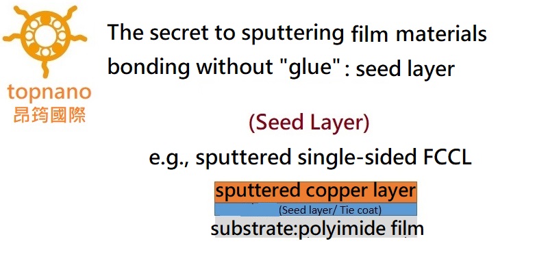
The following uses sputtered flexible copper foil substrate (FCCL) as an example to illustrate the function of the seed layer:
Since the substrate of the flexible copper foil substrate is an insulator such as a polyimide film (PI film), the copper conductor layer cannot be directly fabricated through electroplating. Therefore, a seed layer tens of nanometers thin is first formed on the substrate film using metals such as nickel (Ni) or chromium (Cr) through sputtering.
Besides serving as the cathode in the subsequent electroplating process, the seed layer also functions to stabilize the adhesion strength between the conductor (e.g., copper) and the substrate film (e.g., PI/PET film) (similar to an adhesive). After the seed layer is formed, subsequent copper electroplating processes can achieve the same reliable and stable adhesion characteristics as the process of manufacturing electrolytic copper foil.
*For more Q&A about roll-to-roll sputtering, please see the <Frequently Asked Questions> at the top of the official website.
*For more Q&A about roll-to-roll sputtering, please see the FAQ at the top of the official website